New Report Identifies Target Areas for CHIPS R&D Investments
Thursday, Oct 27, 2022, 5:00am
by Semiconductor Industry Association
SIA-BCG study calls for new federal funds to be directed at five key areas of semiconductor R&D
WASHINGTON, Oct. 27, 2022—Following landmark enactment in August 2022 of the CHIPS and Science Act to reinvigorate domestic semiconductor manufacturing and research, the Semiconductor Industry Association (SIA) and the Boston Consulting Group (BCG) today released a report identifying five key areas of the semiconductor R&D ecosystem that should be strengthened by the new law’s R&D funding.
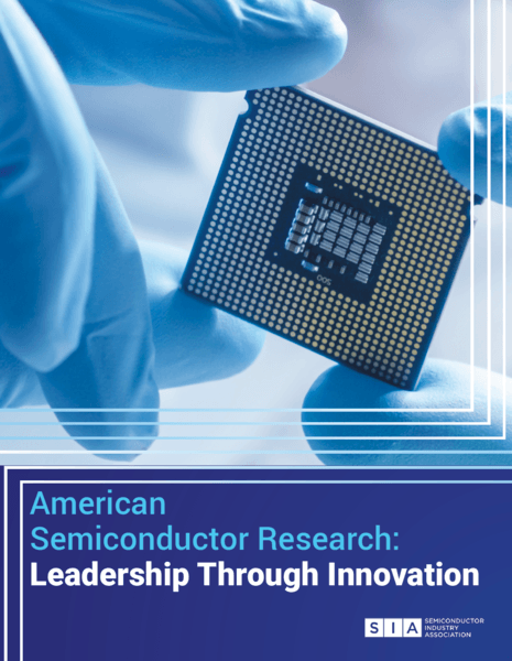
 The report, titled “American Semiconductor Research: Leadership Through Innovation,” highlights the importance of government-industry collaboration on two historic new entities—the National Semiconductor Technology Center (NSTC) and the National Advanced Packaging Manufacturing Program (NAPMP)—created by the CHIPS and Science Act. The study also calls for CHIPS funding to be used to bridge key gaps in the current semiconductor R&D ecosystem. Doing so will help pave the way for sustained U.S. chip innovation leadership, according to the report.
[DOWNLOAD THE REPORT]
“Semiconductor R&D is essential to the innovations powering America’s economy, national security, advanced manufacturing, and critical supply chains,” said John Neuffer, SIA president and CEO. “Enactment of the CHIPS and Science Act was a major step toward reinvigorating domestic chip production and innovation for years to come. The ‘Leadership Through Innovation’ study is a roadmap for implementing the new law’s R&D provisions and ensuring sustained U.S. leadership in chip technology.”
Based on our extensive consultations with industry technology leaders, the report calls for bolstering the U.S. R&D ecosystem’s capabilities through investments in five key areas:
(1) Transitioning and Scaling Pathfinding Research
- The NSTC and NAPMP should serve to bridge the gap between early-stage R&D and at-scale production. Both should strengthen the R&D ecosystem’s ability to conduct R&D and commercialize technologies that are 5 to 15 years from production.
- The NSTC and NAPMP can become hubs for aligning R&D efforts, both for industry and government agencies, allowing industry to participate in programs where it has interests, and enabling agencies to focus their own funds on their respective missions.
(2) Research Infrastructure and (3) Development Infrastructure
- The NSTC and NAPMP should play an active role in expanding, upgrading, and providing access to institutions’ technology development capabilities where they align with R&D priorities. The two initiatives must neither spread funding too thinly nor concentrate investments in a single technology or location. Rather, both must balance the benefits of a highly distributed network against the benefits of scale, based on technology needs.
- Specifically, it is critical the NSTC and NAPMP use existing infrastructure where possible to leverage CHIPS funding and enable faster learnings by benefiting from available resources.
- The primary support the NSTC and NAPMP will provide for research efforts is the establishment of transition paths for promising technologies through prototyping and scale-up.
(4) Collaborative Development
- The NSTC and NAPMP should support full-stack innovation by convening companies to solve complex technological problems that benefit from collaboration across the full computing stack and accelerate the development of technologies, tools, and methodologies.
- For example, creating next-generation data centers requires bringing together expertise in advanced materials, new computing architectures, packaging, software, and more.
- In particular, the NAPMP can convene technical experts to provide input to organizations like Institute of Electrical and Electronics Engineers (IEEE) and Joint Electron Device Engineering Council (JEDEC) when developing, for example, integration standards for heterogenous integration, chiplets, and other components of secure technologies.
(5) Workforce
- The NSTC and NAPMP should promote a range of programs that expand the size and skills of the U.S. semiconductor R&D pipeline and workforce to strengthen the U.S. R&D ecosystem and the economic competitiveness it underpins.
- Without these efforts, the inadequate supply of highly skilled R&D workers – those in semiconductor design, manufacturing, and the other activities of the value chain – threatens to limit the pace of innovation.
# # #
Media Contact
Dan Rosso
Semiconductor Industry Association
240-305-4738
drosso@semiconductors.org
About SIA
The Semiconductor Industry Association (SIA) is the voice of the semiconductor industry, one of America’s top export industries and a key driver of America’s economic strength, national security, and global competitiveness. SIA represents 99% of the U.S. semiconductor industry by revenue and nearly two-thirds of non-U.S. chip firms. Through this coalition, SIA seeks to strengthen leadership of semiconductor manufacturing, design, and research by working with Congress, the Administration, and key industry stakeholders around the world to encourage policies that fuel innovation, propel business, and drive international competition. Learn more at www.semiconductors.org.
